Research:Photonic waveguide circuit integrated with carbon nanotube single-photon source operating at room temperature
Currently a rapidly growing research field at the heart of many emerging technologies, photonic integrated circuits (PIC) have enabled the realization of mass-manufacturable, stable, resilient and compact optical circuits for a large panel of applications. However, quantum photonic integrated circuits development has remained limited due to the lack of scalable chip-integration techniques for implementing quantum light sources generating single photons at room temperature. Carbon nanotubes (CNTs) have been proposed as promising candidates but have yet to be demonstrated in functional quantum photonics circuits due to the stringent conditions indispensable for producing and manipulating photons with pure states. In this research we aim to develop such tools as a technological starting point for CNT-based quantum PIC applications.
Firstly, as a result of thorough excitonic analysis involving spectral, lifetime, polarization, photoluminescence(PL) and autocorrelation measurements, (6,5)carbon-nanotubes with single defects have firstly been identified as a promising choice for chip integration.
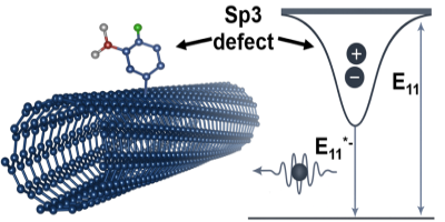

A photonic integrated circuit characterization platform has been realized and implemented to a photoluminescence measurement set-up for CNT circuit coupling analysis. Following, different types of photonic circuit fabrication processes have been developed in cleanroom and used to realize a large variety of photonic nanostructures such as couplers, resonators, interferometers, waveguides, gratings or cavities. CNTs have then been implemented both by drop-casting or deterministic positioning techniques such as anthracene stamping and coupled to these circuits on grating cavities.

This allows Purcell effect enhancement, demonstrating a sharpened and magnified photon-emission into waveguides. Finally, we also showed single-photon emission at room temperature and waveguide photonic coupling of a deterministically positioned CNT in a lithium niobate waveguide circuit, readily available for electro-optical modulator processing.

To learn more about this work, please refer to:
Photonic Waveguide Circuit Integrated with Carbon Nanotube Single-Photon Source Operating at Room Temperature
ACS Photonics
13, 4539 (2026).
