Research:High efficiency coupling of individual carbon nanotubes to photonic crystal nanobeam cavities
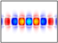
Photonic crystal nanocavities confine light by inserting a defect into a structure with periodic modulation of index of refraction. In a photonic crystal nanobeam, a periodic array of air holes is etched into a waveguide to form a photonic bandgap, which acts as a Bragg reflector. There are two types of cavity modes known as dielectric modes and air modes. The dielectric modes have large fields in the dielectric material, while the air modes have large fields in the air. Electric-field profile of an air mode is shown below.

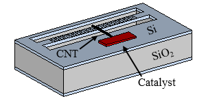
Because nanotube luminescence is quenched when they are in contact with the substrate, there is a possibility for more efficient optical coupling by using the air modes. Here we have investigated optical coupling between air-suspended carbon nanotubes and photonic crystal nanobeam cavities.
Photonic crystal nanobeam cavities are fabricated from silicon-on-insulator (SOI) substrates. First, we perform electron beam lithography to pattern the nanobeam with an array of holes on the resist. The resist is developed and the photonic crystal structure is formed by dry etching. Next, the burried oxide layer is removed by wet etching. Finally, carbon nanotubes are grown onto the cavity by chemical vapor deposition.

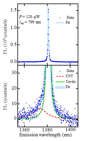
We have performed photoluminescence measurements on such devices, and confirmed very sharp peak at emission wavelengths of nanotubes. On one of the devices, we have observed very efficient coupling between the nanotube and the cavity such that the original spectrum of nanotubes is barely visible. This is in contrast to the case of silicon microdisk resonators. By performing an analysis, we estimate that 85% of the emitted light couples to the cavity.

To learn more about this work, please refer to:
Ultralow mode-volume photonic crystal nanobeam cavities for high-efficiency coupling to individual carbon nanotube emitters
Nature Commun.
5, 5580 (2014).
![]()