Research:Carbon-nanotube field-effect transistor
Single-walled carbon nanotubes have diameters of only a few nanometers, but they can grow as long as a millimeter. It is very difficult to put electrical contacts on a molecule or a quantum dot, but in the case of carbon nanotubes, it is fairly easy to make a device with individual nanotubes.
Field effect transistors (FETs) are an example of such devices. By applying gate voltages, conductivity of a nanotube can be modulated. Here we will discuss back-gated field effect transistor fabricated on a Si substrate with a thermal oxide layer.
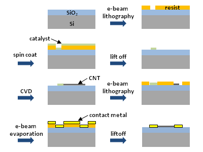
Device fabrication starts by placing catalyst where we want to grow carbon nanotubes. Catalyst solution is spin-coated and lifted off. Then chemical vapor deposition is performed to grow carbon nanotubes. Finally, metal contacts are evaporated.
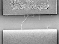
It is possible to make transistors with individual carbon nanotubes by carefully adjusting the catalyst composition and amount, as well as other growth conditions. If a transistor is made from a single nanotube, its electrical characteristics allow the determination of whether the nanotube is metallic or semiconducting.