Research:Hexagonal boron nitride as an ideal substrate for carbon nanotube photonics
Hexagonal boron nitride (h-BN), a two-dimensional (2D) material, is atomically flat with low defect density, which is widely used to support other 2D materials for both electronics and photonics. We expect that the advantages of h-BN can also be utilized in mixed dimensional heterostructures, and carbon nanotubes (CNTs) would provide a unique opportunity in this context. The one-dimensional nature of CNTs results in enhanced Coulomb interactions, giving rise to tightly bound excitons that show photoluminescence (PL) at room temperature. CNTs directly attached on solid-state substrates such as SiO2/Si, however, suffers from the strong substrate quenching effect, hindering applications in all-solid-state optical devices. By using h-BN as a substrate, the quenching effect is expected to be suppressed. Moreover, excitons in CNTs are sensitive to the dielectric environment, and intimate contact with the 2D h-BN substrate could result in large modifications in excitonic energies.
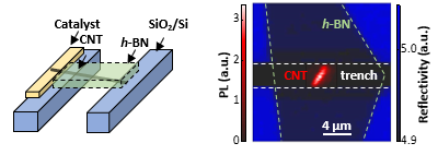
Here we study h-BN effects on PL excitation (PLE) spectra of CNTs by transferring h-BN flakes over air-suspended CNTs grown over trenches on SiO2/Si substrates. The reflectivity image of h-BN and the PL image of CNT depict the shape of h-BN/CNT heterostructure.
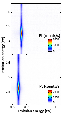
A clean PLE map can be obtained even after the transfer, since the PL intensity remains sufficiently strong. The reduction ratio of PL intensity after transfer compared to before transfer averages to 0.48, while the PL reduction ratio is typically less than 0.01 in the current solid-state substrates such as SiO2/Si, quartz, and metals. We point out that the full width at half-maximum for E11 emission shows only a slight increase by 2.2 meV. The line width of h-BN/CNT is much smaller than CNTs on other solid-state substrates. The small change in the line width at room temperature suggest that our 1D/2D heterostructures show comparable interfacial properties to 2D/2D heterostructures.
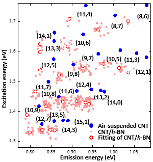
The PLE maps also show substantial modifications of the excitonic energies. In order to obtain statistical information from the ensemble of CNTs, we have collected more than 400 PLE maps from the CNT/h-BN samples. Large redshifts in E11 and E22 of ~50 meV are observed, which is difficult to explain by the dielectric screening effect alone.
To learn more about this work, please refer to:
Hexagonal boron nitride as an ideal substrate for carbon nanotube photonics
ACS Photonics
7, 1773 (2020).
