Research:Self-aligned hybrid nanocavities using atomically thin materials
Two-dimensional (2D) van der Waals layered materials are increasingly being adopted in hybrid photonics. The 2D materials are often integrated with photonic structures including cavities to enhance light-matter coupling, providing additional control and functionality. The conventional approach to hybrid devices involves the transfer of 2D material mono- and few-layer flakes onto prefabricated nanocavities. Despite being ultrathin, the transfer of a 2D material flake could alter the dielectric environment of the cavity. Interestingly, the impact of the flake on the dielectric environment is usually ignored or regarded as a small perturbation that only needs to be slightly compensated for by adjusting the design of the nanophotonic cavity. The potential of 2D materials for dielectric environment engineering in hybrid nanophotonic devices is still largely unexplored. Instead of being a detriment, the change in the dielectric environment caused by the 2D material can be utilized to enable alternative methods for enhanced cavity light-matter coupling.
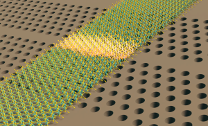
In our work, we demonstrate a novel method to the form high Q factor nanocavities by partially covering a photonic crystal (PhC) waveguide post-fabrication with a suitably-sized 2D material flake. The presence of the flake increases the local refractive index and in turn decreases the frequency of the guided modes. The frequency mismatch of the optical fields in the regions with and without the flake results in the formation of a nanocavity. We successfully fabricated such hybrid nanocavity devices with hBN, WSe2 and MoTe2 flakes on silicon PhC waveguides, obtaining Q factors as high as 4.0×10⁵. Remarkably, even monolayer flakes can provide sufficient local refractive index modulation to induce high Q nanocavity formation. We have also managed to observe cavity PL enhancement in a self-aligned MoTe2 cavity device, with a cavity Purcell enhancement factor of about 15.
Our results demonstrate the utility of 2D materials for dielectric environment engineering to create functional hybrid devices, with potential applications in hybrid integrated photonic circuits. This versatile approach can be extended to a wide variety of materials, with further room for more complex material and photonic engineering to manipulate light-matter interaction. Therefore, our results will have a significant impact on numerous fields including layer materials nanoscience, hybrid device applications and integrated photonics.
To learn more about this work, please refer to
Self-aligned hybrid nanocavities using atomically thin materials
ACS Photonics
11, 2247 (2024).
