Research:Deterministic transfer of optical-quality carbon nanotubes for atomically defined technology
Miniaturization of electronic devices has been a driving force for technological innovation. In the not-too-distant future, tiny materials with atomically defined structures and interfaces may become the building blocks of devices. In two-dimensional van der Waals heterostructures, for example, materials with defined at the atomic level are stacked with their layer number and rotation angle well controlled, giving rise to various new physical phenomena. Atoms and molecules, tiny components that have fixed structures, can provide a higher degree of freedom as building blocks, but they are difficult to manipulate and hold at room temperature and in air. Although the integration of semiconductor nanostructures into electronic and photonic devices is feasible, it remains a challenge to reproducibly prepare identical structures.
In this context, carbon nanotubes are the ideal candidate for building atomically defined technology. It has been possible to find a single carbon nanotube with the desired chirality and build transistors and light-emitting devices out of it. However, to combine carbon nanotubes with other nanomaterials for higher-order functionalities and their integration, a technology to precisely manipulate nanotubes is desired. Here we have developed a technique for transferring clean nanotubes to a desired location by using a single crystal of anthracene as a medium. By monitoring bright luminescence of nanotubes supported on an anthracene crystal, we can place a nanotube of desired chirality with high spatial precision.
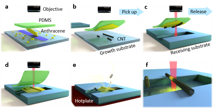
When growing nanotubes on a single-crystalline quartz substrate, the interaction with the substrate surface allows for long growth in a specific direction, but due to this strong interaction, almost no fluorescence can be detected from nanotubes. After transferring such nanotubes onto trenches with our technique, we observe ~5000X brighter fluorescence. This is comparable to that of as-grown suspended nanotubes, indicating the possibility of using arrays of such long carbon nanotubes in light-emitting devices.
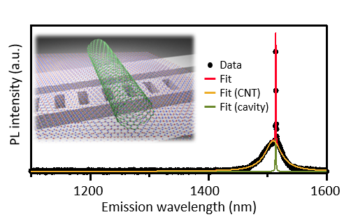
Also, it is important to spatially and spectrally couple carbon nanotubes to optical microcavities and waveguides in photonic circuits. We demonstrate the deterministic coupling of a single nanotube to a photonic crystal nanobeam cavity. To overcome the shortcomings of carbon nanotubes, whose fluorescence is lost when in contact with normal solid substrates, we use ~30nm-thick hexagonal boron nitride as a spacer. The boron nitride also prevents the decay of the electric field enhanced by the nanobeam. The compatibility of our transfer technique with one-dimensional and two-dimensional materials is also a key for this device fabrication. By precisely manipulating carbon nanotubes with a specific chirality and freely combining them with nanostructures and other low-dimensional materials, we should be able to pave the way for the construction of devices with new functionalities.
To learn more about this work, please refer to:
Deterministic transfer of optical-quality carbon nanotubes for atomically defined technology
Nature Commun.
12, 3138 (2021).

RIKEN Press Release:
"Engineering matter at the atomic level"
(Related article in
RIKEN Research, Fall 2021
)
Review article:
Deterministic manipulation of carbon nanotubes for optical devices
JSAP Review
2023, 230406 (2023).